Doping is a process used in semiconductor materials to intentionally introduce impurities into the material in order to alter its electrical properties. Doping is a crucial step in the manufacture of various electronic devices, including transistors, diodes, solar cells, and LEDs.
Semiconductors are materials with properties that are intermediate between those of conductors (such as metals) and insulators (such as glass or rubber). At room temperature, pure semiconductors have very few free electrons, making them poor conductors of electricity. However, the addition of impurities or dopants can significantly alter the electrical properties of the material, making it more conductive or less conductive.
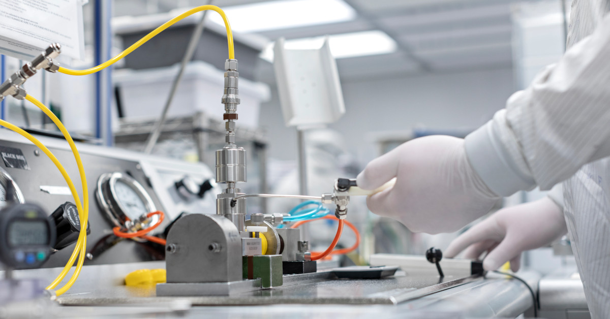
Dopants are typically introduced into the semiconductor material by a process called ion implantation or diffusion. In ion implantation, ions of the dopant material are accelerated to high speeds and then implanted into the semiconductor material. In diffusion, the dopant material is diffused into the semiconductor material by heating the material in the presence of the dopant material.
The choice of dopant material depends on the desired electrical properties of the semiconductor. Dopants that add extra electrons to the semiconductor material are called n-type dopants, and those that remove electrons from the material are called p-type dopants. The most commonly used n-type dopant is phosphorus, while the most commonly used p-type dopant is boron.
When a dopant is added to a semiconductor material, it creates an excess of either electrons or holes (the absence of electrons) in the material. In n-type semiconductors, the dopant atoms have extra electrons that are free to move around the material. These free electrons are called minority carriers, and they contribute to the material’s electrical conductivity. In p-type semiconductors, the dopant atoms have fewer electrons than the semiconductor material, leaving “holes” in the material. These holes are also minority carriers and contribute to the material’s electrical conductivity.
The behavior of semiconductors doped with both n-type and p-type dopants is used to create p-n junctions, which are the basis of many electronic devices. A p-n junction is created by placing a p-type material next to an n-type material. The junction between the two materials forms a depletion region, which is an area where the majority carriers (electrons in the n-type material and holes in the p-type material) have recombined, leaving behind only the minority carriers. The depletion region acts as a barrier to the flow of current in the absence of an external voltage.
When a voltage is applied across a p-n junction, it can cause the depletion region to shrink or disappear, allowing current to flow through the junction. This effect is used in many electronic devices, including diodes, transistors, and solar cells. In a diode, for example, the p-n junction acts as a one-way valve for electrical current, allowing current to flow in one direction but not the other. In a transistor, the voltage applied to the p-n junction controls the flow of current through the device.
Doping is a critical process in semiconductor manufacturing that allows the electrical properties of the material to be precisely controlled. By adding dopants to a semiconductor material, the conductivity of the material can be adjusted, allowing it to be used in a wide range of electronic devices. The behavior of p-n junctions, which are formed by doping a semiconductor with both p-type and n-type dopants, is the basis of many electronic devices, including diodes, transistors, and solar cells. We will go over the p-n junction next.
Leave a Reply